The Advantages of Modular System Architecture
Alex Ko, Technical Advisor
The semiconductor industry is going through a paradigm shift, quickly reaching the limits of what will fit into a single packaged chip. The latest methods to enable more computing within one package include adopting advanced packaging methods, as seen in the latest GPUs with High Bandwidth Memory (HBM) onboard the same package, like those used for AI training and inference. Challenges with manufacturing these AI processors are driving the need for new technologies in semiconductor Inspection and Metrology (I&M). Advanced packaging methods used in this process consist of stacking chiplets on top of chiplets, or chips on top of interposers. As more layers are stacked, each step increases the money invested in completing the devices. However, current inspection technologies used in production cannot easily see between the layers to validate if they are aligned or bonded correctly. If defects between the layers can be found early, there is a chance to repair them or to stop investing in adding more components (cost) to the device. Chip makers are calling for faster commercialization of state-of-the-art technologies to help them see between these layers, improving their yield and lowering costs.
New Players in Town
Some new I&M methods are developed at startups, universities, or national labs that may not have the background to commercialize these technologies into production-ready systems. Some development groups within established top-tier semiconductor equipment companies may be working on a beta system for early process integration into an R&D fab. They all tend to have something in common-they have a new enabling technology but don't have the know-how, infrastructure, or resources to commercialize it into a system that complies with industry standards for fully automated semiconductor manufacturing equipment.
How Do They Get to Market?
In the past, companies have typically followed a few paths forward:
- adapt an existing system to support the new technology,
- build an in-house engineering team and create the manufacturing infrastructure from scratch, or
- partner with an external engineering firm to design and build a custom system tailored to their needs.
In many cases, these groups do not have the benefit of access to an existing system to leverage. However, those who do can find a donor system to be cumbersome, as all interfaces and system infrastructure are optimized for a different process. This approach can make retrofitting difficult, time-consuming, and expensive with the new technology.
Those who have the budget to hire an in-house team and build out the manufacturing infrastructure can be under time pressure to deliver the first units for validation on a pilot line. Hiring alone can take 6 months to more than a year to find candidates with the appropriate background and ramp them up to being fully productive. There is also manufacturing infrastructure that may need to be built, such as clean rooms, electrical panels, and gas lines, often impacted by permits. This approach can delay the delivery of the first units beyond the window of opportunity for customer qualification.
External engineering services companies have been the path of choice for many of these groups that have a technology to commercialize. Leveraging an existing engineering team and manufacturing infrastructure is often the most effective approach for companies in these situations. After aligning on the performance requirements, the design can be completed and optimized for this new technology, using the existing knowledge and infrastructure from a company that already has the expertise and the cleanroom ready for integration and testing. This is often the fastest path to a production-ready system that meets end-user requirements and complies with industry standards.
Modular System: A New Path to Commercialization
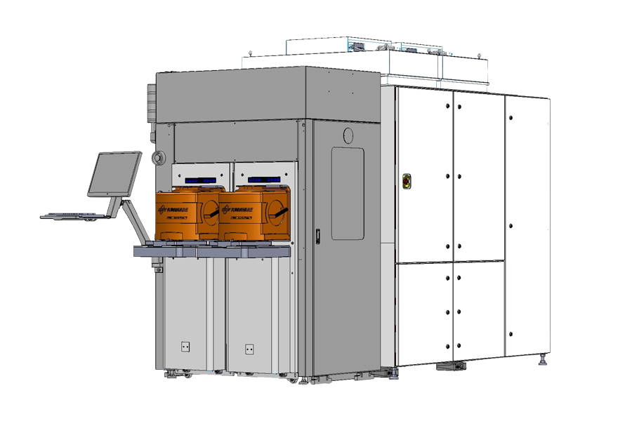
A new option has been introduced to further enhance the already fast time-to-market that Owens Design delivers. PR:IME™ is a pre-engineered platform with modular interfaces across software, mechanical, and electrical components. With designs and specifications already completed for the long lead time items (LLIs), these can be ordered on day one without starting from scratch on a custom design. By fully leveraging this modular architecture, companies can save on project timelines, saving 20% to 50% compared to a full custom design. By adopting a modular architecture, a "plug & play" system can be available for quick and seamless integration of new technologies into a production-ready product - shippable in record time.
Lowering Risk
Whenever a new design is introduced, there runs some risk of debugging being required. By utilizing a modular design that has been proven across multiple products, the risks associated with new system-level components and assemblies are significantly reduced. Only a small portion remains when most of the system has already been validated, allowing for more focused and thorough scrutiny of limited customizations.
Leveraging Common Materials
A modular design with standard components allows customers to take advantage of pre-negotiated lead times. In some cases, it also helps lower the risk of supplier errors that can occur when producing a custom part for the first time. By using the same parts across multiple systems, suppliers can refine their processes to improve yields and quality over time.
Time is Money
Startups are particularly sensitive to non-recurring engineering (NRE) costs and company burn rate. Extra time spent in development not only incurs cost for NRE, but it also burns through valuable runway for the companies while they wait to launch their product. One additional iteration of a design or a delayed delivery has the potential to jeopardize a startup's business. Being able to speed up development not only reduces the product costs but also saves the company in their burn rate multiplied by their time savings. Leveraging a proven, ready-to-integrate modular system shortens productization time, lowers risk, and ultimately preserves more runway for startups to succeed.
Changing the Industry
Global fab customers have made the call to ask for new I&M technologies to help them advance AI processor manufacturing and drive prices down. The industry has responded, developing new technologies to bridge these gaps in production capabilities. But they need a fast path to get to market. As a trusted leader, Owens Design has played a key role in this, helping companies bring new semiconductor solutions to fabs. Now PR:IME™ is taking it a step ahead - improving on the already world-class lead times to drive even faster technology commercialization.
